
Graphene is a one-atom-thick planar sheet of sp2-bonded carbon atoms that are densely packed in a honeycomb crystal lattice. It can be visualized as an atomic-scale chicken wire made of carbon atoms and their bonds. The name comes from graphite + -ene; graphite itself consists of many graphene sheets stacked together.
The carbon-carbon bond length in graphene is about 0.142 nm. Graphene is the basic structural element of some carbon allotropes including graphite, carbon nanotubes and fullerenes. It can also be considered as an infinitely large aromatic molecule, the limiting case of the family of flat polycyclic aromatic hydrocarbons called graphenes. The Nobel Prize in Physics for 2010 was awarded to Andre Geim and Konstantin Novoselov "for groundbreaking experiments regarding the two-dimensional material graphene".


Description
A simple, non-technical definition has been given in a recent review on graphene:
Graphene is a flat monolayer of carbon atoms tightly packed into a two-dimensional (2D) honeycomb lattice, and is a basic building block for graphitic materials of all other dimensionalities. It can be wrapped up into 0D fullerenes, rolled into 1D nanotubes or stacked into 3D graphite.
Previously, graphene was also defined in the chemical literature as follows:
A single carbon layer of the graphitic structure can be considered as the final member of the series naphthalene, anthracene, coronene, etc. and the term graphene should therefore be used to designate the individual carbon layers in graphite intercalation compounds. Use of the term "graphene layer" is also considered for the general terminology of carbons.
The IUPAC compendium of technology states: "previously, descriptions such as graphite layers, carbon layers, or carbon sheets have been used for the term graphene...it is not correct to use for a single layer a term which includes the term graphite, which would imply a three-dimensional structure. The term graphene should be used only when the reactions, structural relations or other properties of individual layers are discussed." In this regard, graphene has been referred to as an infinite alternant (only six-member carbon ring) polycyclic aromatic hydrocarbon (PAH). The largest molecule of this type consists of 222 atoms and is 10 benzene rings across. It has proven difficult to synthesize even slightly bigger molecules, and they still remain "a dream of many organic and polymer chemists". Furthermore, ab initio calculations show that a graphene sheet is thermodynamically unstable with respect to other fullerene structures if its size is less than about 20 nm (“graphene is the least stable structure until about 6000 atoms” and becomes the most stable one (as within graphite) only for sizes larger than 24,000 carbon atoms). The flat graphene sheet is also known to be unstable with respect to scrolling, which is its lower energy state.
Also, a definition of "isolated or free standing graphene" has recently been proposed: "graphene is a single atomic plane of graphite, which—and this is essential—is sufficiently isolated from its environment to be considered free-standing." This definition is narrower than the definitions given above and refers to cleaved, transferred and suspended graphene monolayers. Other forms of graphene, such as graphene grown on various metals, can also become free-standing if transferred to, e.g., SiO2 or suspended. A new example of isolated graphene is graphene on SiC after its passivation with hydrogen,.
Graphene and Occurrence and production,
Graphene is essentially an isolated atomic plane of graphite. Therefore, from this perspective, graphene has been known since the invention of X-ray crystallography. Graphene planes become even better separated in intercalated graphite compounds. In 2004 physicists from University of Manchester and Institute for Microelectronics Technology, Chernogolovka, Russia, found a way to isolate individual graphene planes by using Scotch tape and they also measured electronic properties of the obtained flakes and showed their fantastic quality. In 2005 the same Manchester group together with researchers from the Columbia University (see the History chapter below) demonstrated that quasiparticles in graphene were massless Dirac fermions. These discoveries led to the explosion of interest in graphene.
Since then, hundreds of researchers have entered the area and, naturally, they carried out the extensive search for relevant earlier papers. The first literature review was given by the Manchester pioneers themselves. They cite several papers in which graphene or ultra-thin graphitic layers were epitaxially grown on various substrates. Also, they point out at a number of pre-2004 reports in which intercalated graphite compounds were studied in a transmission electron microscope. In the latter case, researchers occasionally observed extremely thin graphitic flakes ("few-layer graphene" and possibly even individual layers). An early detailed study on few-layer graphene dates back to 1962. The earliest TEM images of few-layer graphene were published by G. Ruess and F. Vogt in 1948. However, already D.C. Brodie was aware of the highly lamellar structure of thermally reduced graphite oxide in 1859. It was studied in detail by V. Kohlschütter and P. Haenni in 1918, who also described the propertites of graphite oxide paper.
It is now well known that tiny fragments of graphene sheets are produced (along with quantities of other debris) whenever graphite is abraded, such as when drawing a line with a pencil. There was little interest in this graphitic residue before 2004/05 and, therefore, the discovery of graphene is often attributed to Andre Geim and colleagues who introduced graphene in its modern incarnation, although it may be argued that this is no more accurate than attributing the discovery of America to Columbus.
In 2008 graphene produced by exfoliation was one of the most expensive materials on Earth, with a sample that can be placed at the cross section of a human hair costing more than $1,000 as of April 2008 (about $100,000,000/cm2). Since then, exfoliation procedures were scaled up, and now companies sell graphene by the ton. On the other hand, the price of epitaxial graphene on silicon carbide is dominated by the substrate price, which is approximately $100/cm2 as of 2009. Even cheaper graphene has been produced by transfer from nickel by Korean researchers, with wafer sizes up to 30" reported.
In the literature, specifically that of the surface science community, graphene has also been commonly referred to as monolayer graphite. This community has intensely studied epitaxial graphene on various surfaces (over 300 articles prior to 2004). In some cases, these graphene layers are coupled to the surfaces weakly enough (by Van der Waals forces) to retain the two dimensional electronic band structure of isolated graphene, as also happens with exfoliated graphene flakes with regard to silicon dioxide. An example of weakly coupled epitaxial graphene is the one grown on silicon carbide (see below),.
Graphene and Drawing method,
In 2004, the British researchers obtained graphene by mechanical exfoliation of graphite. They used Scotch tape to repeatedly split graphite crystals into increasingly thinner pieces. The tape with attached optically transparent flakes was dissolved in acetone and, after a few further steps, the flakes including monolayers were sedimented on a Si wafer. Individual atomic planes were then hunted in an optical microscope. A year later, the researchers simplified the technique and started using dry deposition, avoiding the stage when graphene floated in a liquid. Relatively large crystallites (first, only a few microns in size but, eventually, larger than 1 mm and visible by a naked eye) were obtained by the technique. It is often referred to as a scotch tape or drawing method. The latter name appeared because the dry deposition resembles drawing with a piece of graphite. The key for the success probably was the use of high throughput visual recognition of graphene on a proper chosen substrate, which provides a small but noticeable optical contrast. For an example of what graphene looks like, see its photograph below.
The isolation of graphene led to the current research boom. Previously, free-standing atomic planes were often "presumed not to exist" because they are thermodynamically unstable on a nm scale and, if unsupported, have a tendency to scroll and buckle. It is currently believed that intrinsic microscopic roughening on the scale of 1 nm could be important for the stability of purely 2D crystals.
It is interesting to note (see Talk:Graphene) that there were a number of previous attempts to make atomically thin graphitic films by using exfoliation techniques similar to the drawing method. Multilayer samples down to 10 nm in thickness were obtained. These efforts were reviewed in. Furthermore, a couple of very old papers were recently unearthed, in which researchers tried to isolate graphene, starting with intercalated compounds (see History and experimental discovery). These papers reported the observation of very thin graphitic fragments (possibly, monolayers) by transmission electron microscopy. Neither of the earlier observations was sufficient to "spark the graphene gold rush", until the Science paper did so by reporting not only macroscopic samples of extracted atomic planes but, importantly, their unusual properties such as the bipolar transistor effect, ballistic transport of charges, large quantum oscillations, etc. The discovery of such interesting qualities intrinsic to graphene gave an immediate boost to further research, and several groups quickly repeated the initial result and moved further. These breakthroughs also helped to attract attention to other production techniques such as epitaxial growth of ultra-thin graphitic films. In particular, it has later been found that graphene monolayers grown on SiC and Ir are weakly coupled to these substrates (how weakly remains debated) and the graphene-substrate interaction can be passivated further.
Not only graphene but also free-standing atomic planes of boron nitride, mica, dichalcogenides and complex oxides were obtained by using the drawing method. Unlike graphene, the other 2D materials have so far attracted surprisingly little attention,.
Graphene and Epitaxial growth on silicon carbide,
Yet another method is to heat silicon carbide to high temperatures (>1100 °C) to reduce it to graphene. This process produces a sample size that is dependent upon the size of the SiC substrate used. The face of the silicon carbide used for graphene creation, the silicon-terminated or carbon-terminated, highly influences the thickness, mobility and carrier density of the graphene.
Many important graphene properties have been identified in graphene produced by this method. For example, the electronic band-structure (so-called Dirac cone structure) has been first visualized in this material. Weak anti-localization is observed in this material and not in exfoliated graphene produced by the pencil trace method. Extremely large, temperature independent mobilities have been observed in SiC epitaxial graphene. They approach those in exfoliated graphene placed on silicon oxide but still much lower than mobilities in suspended graphene produced by the drawing method. It was recently shown that even without being transferred graphene on SiC exhibits the properties of massless Dirac fermions such as the anomalous quantum Hall effect.
The weak van der Waals forces that provide the cohesion of multilayer graphene stacks do not always affect the electronic properties of the individual graphene layers in the stack. That is, while the electronic properties of certain multilayered epitaxial graphenes are identical to that of a single graphene layer, in other cases the properties are affected as they are for graphene layers in bulk graphite. This effect is theoretically well understood and is related to the symmetry of the interlayer interactions.
Epitaxial graphene on silicon carbide can be patterned using standard microelectronics methods. The possibility of large integrated electronics on SiC epitaxial graphene was first proposed in 2004 by a team researchers at Georgia Tech, lead by Walter de Heer. (A patent for graphene based electronics was applied for in 2003 and issued in 2006). Since then, important advances have been made. In 2008, researchers at MIT Lincoln Lab have produced hundreds of transistors on a single chip and in 2009, very high frequency transistors have been produced at the Hughes Research Laboratories on monolayer graphene on silicon carbide.
Graphene and Epitaxial growth on metal substrates
This method uses the atomic structure of a metal substrate to seed the growth of the graphene (epitaxial growth). Graphene grown on ruthenium doesn't typically yield a sample with a uniform thickness of graphene layers, and bonding between the bottom graphene layer and the substrate may affect the properties of the carbon layers.Graphene grown on iridium on the other hand is very weakly bonded, uniform in thickness, and can be made highly ordered. Like on many other substrates, graphene on iridium is slightly rippled. Due to the long-range order of these ripples generation of minigaps in the electronic band-structure (Dirac cone) becomes visible. High-quality sheets of few layer graphene exceeding 1 cm2 (0.2 sq in) in area have been synthesized via chemical vapor deposition on thin nickel films. These sheets have been successfully transferred to various substrates, demonstrating viability for numerous electronic applications. An improvement of this technique has been found in copper foil where the growth automatically stops after a single graphene layer, and arbitrarily large graphene films can be created,.
Graphene and Hydrazine reduction,
Researchers have developed a method of placing graphene oxide paper in a solution of pure hydrazine (a chemical compound of nitrogen and hydrogen), which reduces the graphene oxide paper into single-layer graphene,.
Graphene and Sodium reduction of ethanol,
A recent publication has described a process for producing gram-quantities of graphene, by the reduction of ethanol by sodium metal, followed by pyrolysis of the ethoxide product, and washing with water to remove sodium salts,.
Graphene and From nanotubes,
Experimental methods for the production of graphene ribbons are reported consisting of cutting open nanotubes. In one such method multi walled carbon nanotubes are cut open in solution by action of potassium permanganate and sulfuric acid. In another method graphene nanoribbons are produced by plasma etching of nanotubes partly embedded in a polymer film,
Graphene Properties,


Graphene and Atomic structure,
The atomic structure of isolated, single-layer graphene was studied by transmission electron microscopy (TEM) on sheets of graphene suspended between bars of a metallic grid. Electron diffraction patterns showed the expected hexagonal lattice of graphene. Suspended graphene also showed "rippling" of the flat sheet, with amplitude of about one nanometer. These ripples may be intrinsic to graphene as a result of the instability of two-dimensional crystals, or may be extrinsic, originating from the ubiquitous dirt seen in all TEM images of graphene. Atomic resolution real-space images of isolated, single-layer graphene on silicon dioxide substrates were obtained by scanning tunneling microscopy. Graphene processed using lithographic techniques is covered by photoresist residue, which must be cleaned to obtain atomic-resolution images. Such residue may be the "adsorbates" observed in TEM images, and may explain the rippling of suspended graphene. Rippling of graphene on the silicon dioxide surface was determined by conformation of graphene to the underlying silicon dioxide, and not an intrinsic effect.
Graphene sheets in solid form (density > 1 g/cm3) usually show evidence in diffraction for graphite's 0.34 nm (002) layering. This is true even of some single-walled carbon nanostructures. However, unlayered graphene with only (hk0) rings has been found in the core of presolar graphite onions. Transmission electron microscope studies show faceting at defects in flat graphene sheets, and suggest a possible role in this unlayered-graphene for two-dimensional dendritic crystallization from a melt,.
Graphene and Electronic properties,
GNR band structure for zig-zag type. Tightbinding calculations show that zigzag type is always metallic.
GNR band structure for arm-chair type. Tightbinding calculations show that armchair type can be semiconducting or metallic depending on width (chirality).
Graphene is quite different from most conventional three-dimensional materials. Intrinsic graphene is a semi-metal or zero-gap semiconductor. Understanding the electronic structure of graphene is the starting point for finding the band structure of graphite. It was realized early on that the E-k relation is linear for low energies near the six corners of the two-dimensional hexagonal Brillouin zone, leading to zero effective mass for electrons and holes. Due to this linear (or “conical") dispersion relation at low energies, electrons and holes near these six points, two of which are inequivalent, behave like relativistic particles described by the Dirac equation for spin 1/2 particles. Hence, the electrons and holes are called Dirac fermions, and the six corners of the Brillouin zone are called the Dirac points. The equation describing the E-k relation is ; where the Fermi velocity vF ~ 106 m/s,.
Graphene and Electronic transport,
Experimental results from transport measurements show that graphene has a remarkably high electron mobility at room temperature, with reported values in excess of 15,000 cm2V−1s−1. Additionally, the symmetry of the experimentally measured conductance indicates that the mobilities for holes and electrons should be nearly the same. The mobility is nearly independent of temperature between 10 K and 100 K, which implies that the dominant scattering mechanism is defect scattering. Scattering by the acoustic phonons of graphene places intrinsic limits on the room temperature mobility to 200,000 cm2V−1s−1 at a carrier density of 1012 cm−2. The corresponding resistivity of the graphene sheet would be 10−6 Ω·cm, less than the resistivity of silver, the lowest resistivity substance known at room temperature. However, for graphene on silicon dioxide substrates, scattering of electrons by optical phonons of the substrate is a larger effect at room temperature than scattering by graphene’s own phonons, and limits the mobility to 40,000 cm2 V−1s−1.
Despite the zero carrier density near the Dirac points, graphene exhibits a minimum conductivity on the order of 4e2 / h. The origin of this minimum conductivity is still unclear. However, rippling of the graphene sheet or ionized impurities in the SiO2 substrate may lead to local puddles of carriers that allow conduction. Several theories suggest that the minimum conductivity should be 4e2 / πh; however, most measurements are of order 4e2 / h or greater and depend on impurity concentration.
Recent experiments have probed the influence of chemical dopants on the carrier mobility in graphene. Schedin et al. doped graphene with various gaseous species (some acceptors, some donors), and found the initial undoped state of a graphene structure can be recovered by gently heating the graphene in vacuum. They reported that even for chemical dopant concentrations in excess of 1012 cm−2 there is no observable change in the carrier mobility. Chen, et al. doped graphene with potassium in ultra high vacuum at low temperature. They found that potassium ions act as expected for charged impurities in graphene, and can reduce the mobility 20-fold. The mobility reduction is reversible on heating the graphene to remove the potassium.
Due to its two-dimensional property, charge fractionalization (where the apparent charge of individual pseudoparticles in low-dimensional systems is less than a single quantum) is thought to occur in graphene. It may therefore be a suitable material for the construction of quantum computers using anyonic circuits,.
Graphene and Optical properties,
Photograph of graphene in transmitted light. This one atom thick crystal can be seen with the naked eye because it absorbs approximately 2.3% of white light, which is π times the fine-structure constant.
Graphene's unique electronic properties produce an unexpectedly high opacity for an atomic monolayer, with a startlingly simple value: it absorbs πα ≈ 2.3% of white light, where α is the fine-structure constant. This is "a consequence of the unusual low-energy electronic structure of monolayer graphene that features electron and hole conical bands meeting each other at the Dirac point ... [which] is qualitatively different from more common quadratic massive bands". Based on the Slonczewski-Weiss-McClure (SWMcC) band model of graphite, the interatomic distance, hopping value and frequency cancel when the optical conductance is calculated using the Fresnel equations in the thin-film limit.
This has been confirmed experimentally, but the measurement is not precise enough to improve on other techniques for determining the fine-structure constant.
Recently it has been demonstrated that the bandgap of graphene can be tuned from 0 to 0.25 eV (about 5 micron wavelength) by applying voltage to a dual-gate bilayer graphene field-effect transistor (FET) at room temperature. The optical response of graphene nanoribbons has also been shown to be tunable into the terahertz regime by an applied magnetic field
Graphene and Saturable absorption,
It is further confirmed that such unique absorption could become saturated when the input optical intensity is above a threshold value. This nonlinear optical behavior is termed saturable absorption and the threshold value is called the saturation fluency. Graphene can be saturated readily under strong excitation over the visible to near-infrared region, due to the universal optical absorption and zero band gap. This has relevance for the mode locking of fiber lasers, where fullband mode locking has been achieved by graphene-based saturable absorber. Due to this special property, graphene has wide application in ultrafast photonics,.
Graphene and Spin transport,
Graphene is thought to be an ideal material for spintronics due to small spin-orbit interaction and near absence of nuclear magnetic moments in carbon. Electrical spin-current injection and detection in graphene was recently demonstrated up to room temperature. Spin coherence length above 1 micron at room temperature was observed, and control of the spin current polarity with an electrical gate was observed at low temperature,.
Graphene and Anomalous quantum Hall effect,
The quantum Hall effect is relevant for accurate measuring standards of electrical quantities, and in 1985 Klaus von Klitzing received the Nobel prize for its discovery. The effect concerns the dependence of a transverse conductivity on a magnetic field, which is perpendicular to a current-carrying stripe. Usually the phenomenon, the quantization of the so-called Hall conductivity σxy at integer multiples of the basic quantity e2 / h (where e is the elementary electric charge and h is Planck's constant) can be observed only in very clean Si or GaAs solids, and at very low temperatures around 3 K, and at very high magnetic fields.
Graphene in contrast, besides its high mobility and minimum conductivity, and because of certain pseudo-relativistic peculiarities to be mentioned below, shows particularly interesting behavior just in the presence of a magnetic field and just with respect to the conductivity-quantization: it displays an anomalous quantum Hall effect with the sequence of steps shifted by 1/2 with respect to the standard sequence, and with an additional factor of 4. Thus, in graphene the Hall conductivity is , where n is the above-mentioned integer "Landau level" index, and the double valley and double spin degeneracies give the factor of 4. Moreover, in graphene these remarkable anomalies can even be measured at room temperature, i.e. at roughly 20 °C. This anomalous behavior is a direct result of the emergent massless Dirac electrons in graphene. In a magnetic field, their spectrum has a Landau level with energy precisely at the Dirac point. This level is a consequence of the Atiyah-Singer index theorem. and is half-filled in neutral graphene, leading to the "+1/2" in the Hall conductivity. Bilayer graphene also shows the quantum Hall effect, but with the standard sequence, i.e. with i.e. with only one of the two anomalies. Interestingly, concerning the second anomaly, the first plateau at N = 0 is absent, indicating that bilayer graphene stays metallic at the neutrality point.
Unlike normal metals, the longitudinal resistance of graphene shows maxima rather than minima for integral values of the Landau filling factor in measurements of the Shubnikov-de Haas oscillations, which show a phase shift of π, known as Berry’s phase. The Berry’s phase arises due to the zero effective carrier mass near the Dirac points. Study of the temperature dependence of the Shubnikov-de Haas oscillations in graphene reveals that the carriers have a non-zero cyclotron mass, despite their zero effective mass from the E-k relation.
Nanostripes: Spin-polarized edge currents
Nanostripes of graphene (in the "zig-zag" orientation), at low temperatures, show spin-polarized metallic edge currents, which also suggests applications in the new field of spintronics. (In the "armchair" orientation, the edges behave like semiconductors.)
Graphene oxide,
Further information: Graphite Oxide,
By disbursing oxidized and chemically processed graphite in water, and using paper-making techniques, the monolayer flakes form a single sheet and bond very powerfully. These sheets, called graphene oxide paper have a measured tensile modulus of 32 GPa. The peculiar chemical property of graphite oxide is related to the functional groups attached to graphene sheets. They even can significantly change the pathway of polymerization and similar chemical processes,.
Graphene and Chemical modification,
Soluble fragments of graphene can be prepared in the laboratory through chemical modification of graphite. First, microcrystalline graphite is treated with a strongly acidic mixture of sulfuric acid and nitric acid. A series of steps involving oxidation and exfoliation result in small graphene plates with carboxyl groups at their edges. These are converted to acid chloride groups by treatment with thionyl chloride; next, they are converted to the corresponding graphene amide via treatment with octadecylamine. The resulting material (circular graphene layers of 5.3 angstrom thickness) is soluble in tetrahydrofuran, tetrachloromethane, and dichloroethane.

Photograph of single-layer graphene oxide undergoing high temperature chemical treatment, resulting in sheet folding and loss of carboxylic functionality, or through room temperature carbodiimide treatment, collapsing into star-like clusters.
Refluxing single-layer graphene oxide (SLGO) in aggressive solvents leads to size reduction and folding of the individual sheets as well as loss of carboxylic group functionality, by up to 20%. This occurs significantly so for hydrazine reduced single-layer graphene oxide (SLGR), by around 60%. Conversion of the remaining carboxylic groups on SLGO or SLGR to acyl chloride intermediates do then react with amines to form amides. Room temperature carbodiimide treatment of SLGO with carbodiimides leads to the collapse of the individual sheets into star-like clusters, which exhibited poor subsequent reactivity with amines. SLGO has also been grafted with polyallylamine, cross-linked through epoxy groups. When filtered into graphene oxide paper, these composites exhibit sheets increased stiffness and strength relative to unmodified graphene oxide paper,.
Full hydrogenation from both sides of graphene sheet results in graphane, but partial hydrogenation leads to hydrogenated graphene,
Graphene and Thermal properties,
The near-room temperature thermal conductivity of graphene was recently measured to be between (4.84±0.44) ×103 to (5.30±0.48) ×103 Wm−1K−1. These measurements, made by a non-contact optical technique, are in excess of those measured for carbon nanotubes or diamond. It can be shown by using the Wiedemann-Franz law, that the thermal conduction is phonon-dominated. However, for a gated graphene strip, an applied gate bias causing a Fermi energy shift much larger than kBT can cause the electronic contribution to increase and dominate over the phonon contribution at low temperatures. The ballistic thermal conductance of graphene is isotropic.
Potential for this high conductivity can be seen by considering graphite, a 3D version of graphene that has basal plane thermal conductivity of over a 1000 W/mK (comparable to diamond). In graphite, the c-axis (out of plane) thermal conductivity is over a factor of ~100 smaller due to the weak binding forces between basal planes as well as the larger lattice spacing.[89] In addition, the ballistic thermal conductance of a graphene is shown to give the lower limit of the ballistic thermal conductances, per unit circumference, length of carbon nanotubes.
Despite its 2-D nature, graphene has 3 acoustic phonon modes. The two in-plane modes (LA, TA) have a linear dispersion relation, whereas the out of plane mode (ZA) has a quadratic dispersion relation. Due to this, the T2 dependent thermal conductivity contribution of the linear modes is dominated at low temperatures by the T1.5 contribution of the out of plane mode. Some graphene phonon bands display negative Grüneisen parameters. At low temperatures (where most optical modes with positive Grüneisen parameters are still not excited) the contribution from the negative Grüneisen parameters will be dominant and thermal expansion coefficient (which is directly proportional to Grüneisen parameters) negative. The lowest negative Grüneisen parameters correspond to the lowest transversal acoustic ZA modes. Phonon frequencies for such modes increase with the in-plane lattice parameter since atoms in the layer upon stretching will be less free to move in the z direction. This is similar to the behavior of a string which is being stretched will have vibrations of smaller amplitude and higher frequency. This phenomenon, named "membrane effect", was predicted by Lifshitz in 1952,.
Graphene and Mechanical properties,
As of 2009, graphene appears to be one of the strongest materials ever tested. Measurements have shown that graphene has a breaking strength 200 times greater than steel. However, the process of separating it from graphite, where it occurs naturally, will require some technological development before it is economical enough to be used in industrial processes, though this may be changing soon.
Using an atomic force microscope (AFM), the spring constant of suspended graphene sheets has been measured. Graphene sheets, held together by van der Waals forces, were suspended over silicon dioxide cavities where an AFM tip was probed to test its mechanical properties. Its spring constant was in the range 1-5 N/m and the Young's modulus was 0.5 TPa, which differs from that of the bulk graphite. These high values make graphene very strong and rigid. These intrinsic properties could lead to using graphene for NEMS applications such as pressure sensors and resonators.
As is true of all materials, regions of graphene are subject to thermal and quantum fluctuations in relative displacement. Although the amplitude of these fluctuations is bounded in 3D structures (even in the limit of infinite size), the Mermin-Wagner theorem shows that the amplitude of long-wavelength fluctuations will grow logarithmically with the scale of a 2D structure, and would therefore be unbounded in structures of infinite size. Local deformation and elastic strain are negligibly affected by this long-range divergence in relative displacement. It is believed that a sufficiently large 2D structure, in the absence of applied lateral tension, will bend and crumple to form a fluctuating 3D structure. Researchers have observed ripples in suspended layers of graphene, and it has been proposed that the ripples are caused by thermal fluctuations in the material. As a consequence of these dynamical deformations, it is debatable whether graphene is truly a 2D structure,.
Graphene and Potential applications,
Graphene and Single molecule gas detection,
Graphene makes an excellent sensor due to its 2D structure. The fact that its entire volume is exposed to its surrounding makes it very efficient to detect adsorbed molecules. Molecule detection is indirect: as a gas molecule adsorbs to the surface of graphene, the location of adsorption experiences a local change in electrical resistance. While this effect occurs in other materials, graphene is superior due to its high electrical conductivity (even when few carriers are present) and low noise which makes this change in resistance detectable,.
Graphene nanoribbons,
Graphene nanoribbons (GNRs) are essentially single layers of graphene that are cut in a particular pattern to give it certain electrical properties. Depending on how the un-bonded edges are configured, they can either be in a zigzag or armchair configuration. Calculations based on tight binding predict that zigzag GNRs are always metallic while armchairs can be either metallic or semiconducting, depending on their width. However, recent density functional theory calculations show that armchair nanoribbons are semiconducting with an energy gap scaling with the inverse of the GNR width.Indeed, experimental results show that the energy gaps do increase with decreasing GNR width. However, as of February 2008, no experimental results have measured the energy gap of a GNR and identified the exact edge structure. Zigzag nanoribbons are also semiconducting and present spin polarized edges. Their 2D structure, high electrical and thermal conductivity, and low noise also make GNRs a possible alternative to copper for integrated circuit interconnects. Some research is also being done to create quantum dots by changing the width of GNRs at select points along the ribbon, creating quantum confinement,.
Graphene transistors,
Due to its high electronic quality, graphene has also attracted the interest of technologists who see them as a way of constructing ballistic transistors. Graphene exhibits a pronounced response to perpendicular external electric fields, allowing one to build FETs (field-effect transistors). In their 2004 paper, the Manchester group demonstrated FETs with a "rather modest" on-off ratio of ~30 at room temperature. In 2006, Georgia Tech researchers announced that they had successfully built an all-graphene planar FET with side gates. Their devices showed changes of 2% at cryogenic temperatures. The first top-gated FET (on-off ratio of <2) was demonstrated by researchers of AMICA and RWTH Aachen University in 2007.Graphene nanoribbons may prove generally capable of replacing silicon as a semiconductor in modern technology.
Facing the fact that current graphene transistors show a very poor on-off ratio, researchers are trying to find ways for improvement. In 2008 researchers of AMICA and University of Manchester demonstrated a new switching effect in graphene field-effect devices. This switching effect is based on a reversible chemical modification of the graphene layer and gives an on-off ratio of greater than six orders of magnitude. These reversible switches could potentially be applied to nonvolatile memories.
In 2009 researchers at the Politecnico di Milano demonstrated four different types of logic gates, each composed of a single graphene transistor. In the same year, the Massachusetts Institute of Technology researchers built an experimental graphene chip known as a frequency multiplier. It is capable of taking an incoming electrical signal of a certain frequency and producing an output signal that is a multiple of that frequency. Although these graphene chips open up a range of new applications, their practical use is limited by a very small voltage gain (typically, the amplitude of the output signal is about 40 times less than that of the input signal). Moreover, none of these circuits was demonstrated to operate at frequencies higher than 25 kHz.
In February 2010, researchers at IBM reported that they have been able to create graphene transistors with an on and off rate of 100 gigahertz, far exceeding the rates of previous attempts, and exceeding the speed of silicon. The 240 nm graphene transistors made at IBM were made using extant silicon-manufacturing equipment, meaning that for the first time graphene transistors are a conceivable—though still fanciful—replacement for silicon,.
Graphene and Integrated circuits,
Graphene has the ideal properties to be an excellent component of integrated circuits. Graphene has a high carrier mobility, as well as low noise, allowing it to be used as the channel in a FET. The issue is that single sheets of graphene are hard to produce, and even harder to make on top of an appropriate substrate. Researchers are looking into methods of transferring single graphene sheets from their source of origin (mechanical exfoliation on SiO2 / Si or thermal graphitization of a SiC surface) onto a target substrate of interest. In 2008, the smallest transistor so far, one atom thick, 10 atoms wide was made of graphene. IBM announced in December 2008 that they have fabricated and characterized graphene transistors operating at GHz frequencies. In May 2009 a team from Stanford University, University of Florida and Lawrence Livermore National Laboratory announced that they have created an n-type transistor, which means that both n and p-type transistors have now been created with graphene. At the same time, the researchers at the Politecnico di Milano demonstrated the first functional graphene integrated circuit – a complementary inverter consisting of one p- and one n-type graphene transistor. However, this inverter also suffered from a very low voltage gain.
According to a January 2010 report from the UK's National Physical Laboratory, a joint group of European research groups epitaxially grew layers on silicon carbide, in a quantity and with quality suitable for mass production of integrated circuits. At high temperatures, the Quantum Hall Effect was accurately measured in these samples by the Quantum Detection Group, a division of the NPL.
See also the 2010 work by IBM in the transistor section above in which they made 'processors' of fast transistors on 2 inch graphene sheets,.
Graphene and Transparent conducting electrodes,
Graphene's high electrical conductivity and high optical transparency make it a candidate for transparent conducting electrodes, required for such applications as touchscreens, liquid crystal displays, organic photovoltaic cells, and organic light-emitting diodes. In particular, graphene's mechanical strength and flexibility are advantageous compared to indium tin oxide, which is brittle, and graphene films may be deposited from solution over large areas.
Large-area, continuous, transparent, and highly conducting few-layered graphene films were produced by chemical vapor deposition and used as anodes for application in photovoltaic devices. A power conversion efficiency (PCE) up to 1.71% was demonstrated, which is 55.2% of the PCE of a control device based on indium-tin-oxide.
Reference material for characterizing electroconductive and transparent materials,
One layer of graphene absorbs 2.3 % of white light. This property was used to define the Conductivity of Transparency that combines the sheet resistance and the transparency. This parameter was used to compare different materials without the use of two independent parameters,.
Graphene and Ultracapacitors,
Due to the incredibly high surface area to mass ratio of graphene, one potential application is in the conductive plates of ultracapacitors. It is believed that graphene could be used to produce ultracapacitors with a greater energy storage density than is currently available,.
Graphene biodevices,
Graphene's modifiable chemistry, large surface area, atomic thickness and molecularly-gatable structure make antibody-functionalized graphene sheets excellent candidates for mammalian and microbial detection and diagnosis devices.
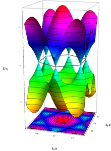
Energy of the electrons with wavenumber k in graphene, calculated in the Tight Binding-approximation. The unoccupied rsp. occupied states, colored in blue-red rsp. yellow-green, touch each other without energy gap exactly at the above-mentioned six k-vectors.
The most ambitious biological application of graphene is for rapid, inexpensive electronic DNA sequencing. Affordable and rapid genome sequencing is widely regarded as the next great frontier for science and will eventually revolutionize personalized medicine and custom medical treatment, enabling doctors to determine genetic susceptibility to a host of diseases and tailor therapies to an individual's genome. Integration of graphene (thickness of 0.34 nm) layers as nanoelectrodes into a nanopore can solve one of the bottleneck issues of nanopore-based single-molecule DNA sequencing,.
Graphene and Anti-bacterial,
The Chinese Academy of Sciences has found sheets of graphene oxide are highly effective at killing bacteria such as Escherichia coli. This means graphene could be useful in applications such as hygiene products or packaging that will help keep food fresh for longer,.
Graphene Pseudo-relativistic theory,
The electrical properties of graphene can be described by a conventional tight-binding model; in this model the energy of the electrons with wavenumber k is.
,
with the nearest-neighbor hopping energy γ0 ≈ 2.8 eV and the lattice constant a ≈ 2.46 Å. Conduction and valence band, respectively, correspond to the different signs in the above dispersion relation; they touch each other in six points, the "K-values". However, only two of these six points are independent, whereas the rest is equivalent by symmetry. In the vicinity of the K-points the energy depends linearly on the wavenumber, similar to a relativistic particle. Since an elementary cell of the lattice has a basis of two atoms, the wave function even has an effective 2-spinor structure. As a consequence, at low energies, even neglecting the true spin, the electrons can be described by an equation which is formally equivalent to the massless Dirac equation. Moreover, in the present case this pseudo-relativistic description is restricted to the chiral limit, i.e., to vanishing rest mass M0, which leads to interesting additional features:
Here vF ~ 106 is the Fermi velocity in graphene which replaces the velocity of light in the Dirac theory; is the vector of the Pauli matrices, is the two-component wave function of the electrons, and E is their energy,.
History of Graphene and experimental discovery,
The term graphene first appeared in 1987 to describe single sheets of graphite as one of the constituents of graphite intercalation compounds (GICs); conceptually a GIC is a crystalline salt of the intercalant and graphene. The term was also used in early descriptions of carbon nanotubes,as well as for epitaxial graphene, and polycyclic aromatic hydrocarbons.
Larger graphene molecules or sheets (so that they can be considered as true isolated 2D crystals) cannot be grown even in principle. An article in Physics Today reads:
"Fundamental forces place seemingly insurmountable barriers in the way of creating [2D crystals] ... Nascent 2D crystallites try to minimize their surface energy and inevitably morph into one of the rich variety of stable 3D structures that occur in soot. But there is a way around the problem. Interactions with 3D structures stabilize 2D crystals during growth. So one can make 2D crystals sandwiched between or placed on top of the atomic planes of a bulk crystal. In that respect, graphene already exists within graphite ... One can then hope to fool Nature and extract single-atom-thick crystallites at a low enough temperature that they remain in the quenched state prescribed by the original higher-temperature 3D growth."
Single layers of graphite were previously (starting from the 1970s) grown epitaxially on top of other materials. This "epitaxial graphene" consists of a single-atom-thick hexagonal lattice of sp2-bonded carbon atoms, as in free-standing graphene. However, there is significant charge transfer from the substrate to the epitaxial graphene, and, in some cases, hybridization between the d orbitals of the substrate atoms and π orbitals of graphene, which significantly alters the electronic structure of the epitaxial graphene.
Single layers of graphite were also observed by transmission electron microscopy within bulk materials (see section Occurrence), in particular inside soot obtained by chemical exfoliation.There have also been a number of efforts to make very thin films of graphite by mechanical exfoliation (starting from 1990 and continuing until after 2004) but nothing thinner than 50 to 100 layers was produced during these years.
A key advance in the science of graphene came when Andre Geim and Kostya Novoselov at Manchester University managed to extract single-atom-thick crystallites (graphene) from bulk graphite in 2004. The Manchester researchers pulled out graphene layers from graphite and transferred them onto thin silicon dioxide on a silicon wafer in a process sometimes called micromechanical cleavage or, simply, the Scotch tape technique. The silicon dioxide electrically isolated the graphene, and was weakly interacting with the graphene, providing nearly charge-neutral graphene layers. The silicon beneath the silicon dioxide could be used as a "back gate" electrode to vary the charge density in the graphene layer over a wide range.
The micromechanical cleavage technique led directly to the first observation of the anomalous quantum Hall effect in graphene, which provided direct evidence of the theoretically predicted pi Berry's phase of massless Dirac fermions in graphene. The anomalous quantum Hall effect in graphene was reported around the same time by Geim and Novoselov and by Philip Kim and Yuanbo Zhang.
Geim has received several awards for his pioneering research on graphene, including the 2007 Mott medal for the "discovery of a new class of materials – free-standing two-dimensional crystals – in particular graphene", the 2008 EuroPhysics Prize (together with Novoselov) "for discovering and isolating a single free-standing atomic layer of carbon (graphene) and elucidating its remarkable electronic properties", and the 2009 Körber Prize for "develop[ing] the first two-dimensional crystals made of carbon atoms". In 2008 and 2009, the Reuters (which also runs a bibliometric service Web of Science) tipped him as one of the front-runners for a Nobel prize in Physics.
The theory of graphene was first explored by Philip R Wallace in 1947 as a starting point for understanding the electronic properties of more complex, 3D graphite. The emergent massless Dirac equation was first pointed out by Gordon W. Semenoff and David P. DeVincenzo and Eugene J. Mele. Semenoff emphasized the occurrence in a magnetic field of an electronic Landau level precisely at the Dirac point. This level is responsible for the anomalous integer quantum Hall effect. Later, single graphene layers were also observed directly by electron microscopy.
More recently, graphene samples prepared on nickel films, and on both the silicon face and carbon face of silicon carbide, have shown the anomalous quantum Hall effect directly in electrical measurements. Graphitic layers on the carbon face of silicon carbide show a clear Dirac spectrum in angle-resolved photoemission experiments, and the anomalous quantum Hall effect is observed in cyclotron resonance and tunneling experiments. Even though graphene on nickel and on silicon carbide have both existed in the laboratory for decades, it was graphene mechanically exfoliated on silicon dioxide that provided the first proof of the Dirac fermion nature of electrons in graphene.
(source:wikipedia)
No comments:
Post a Comment